| CPC H01R 13/6469 (2013.01) [H01R 12/718 (2013.01); H01R 13/6471 (2013.01); H05K 7/1452 (2013.01)] | 20 Claims |
|
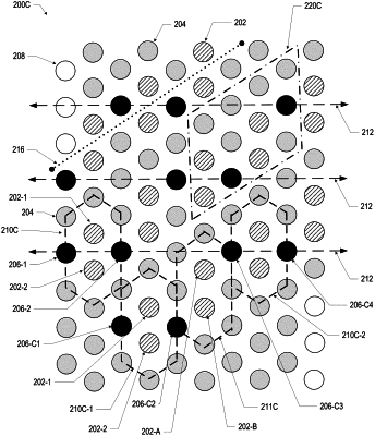
1. A microelectronic device having a hexagonal node configuration, comprising:
a differential signal node pair;
a miscellaneous node;
a power node; and
a plurality of ground nodes; and
wherein the differential signal node pair, the miscellaneous node, the power node, and the plurality of ground nodes are arranged in a hexagonal parallelogon pattern, wherein the differential signal node pair includes a first differential signal node adjacent to a second differential signal node, wherein the power node is adjacent and symmetric to the differential signal node pair, and wherein the miscellaneous node is adjacent and symmetric to the differential signal node pair.
|