| CPC H01R 12/58 (2013.01) [H01R 12/52 (2013.01); H05K 1/18 (2013.01); H05K 3/308 (2013.01); H01R 12/57 (2013.01); H05K 2201/10015 (2013.01); H05K 2201/10166 (2013.01); H05K 2201/10318 (2013.01); H05K 2201/10378 (2013.01); H05K 2201/1059 (2013.01)] | 10 Claims |
|
1. A power electronics arrangement, comprising:
a printed circuit board and
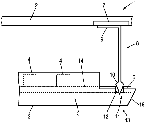
at least one power module fastened on the printed circuit board, wherein the at least one power module has one or more electronic components potted by a potting compound, wherein at least one module connecting point of the at least one power module is electrically contacted with at least one board connecting point of the printed circuit board by an electrically conductive pin, wherein a base section of the electrically conductive pin is fastened on the module connecting point of the at least one power module or on the board connecting point of the printed circuit board, and the end of the electrically conductive pin opposite to the base section, in the installation position, is configured to be pressed, while the at least one power module moves relative to the printed circuit board, into a contacting opening assigned or assignable to the respective other connecting point to implement an electrical contact of these connecting points, wherein the electrically conductive pin, in the installation position, extends linearly from the module connecting point to the board connecting point and is arranged perpendicularly to the printed circuit board surface, wherein the electrically conductive pin is supported on a buttress section that is formed from the potting compound and has the module connecting point.
|