| CPC H01R 12/57 (2013.01) [H01R 4/02 (2013.01); H01R 43/205 (2013.01); H01R 13/22 (2013.01); H05K 1/147 (2013.01); H05K 1/189 (2013.01); H05K 2201/056 (2013.01); H05K 2201/10128 (2013.01)] | 21 Claims |
|
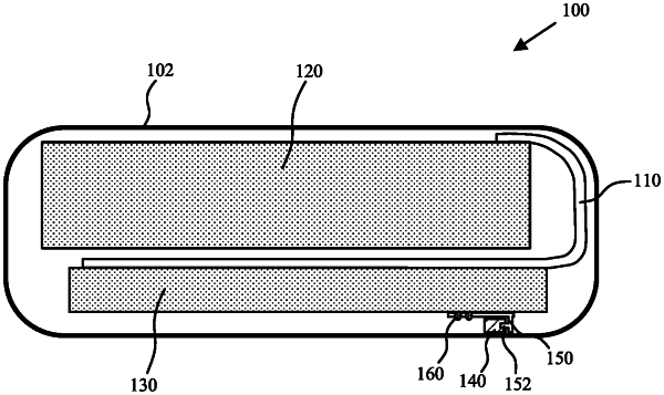
1. An electronic assembly comprising:
a receiving substrate including a landing pad;
a retention structure bonded to the receiving substrate;
wherein the retention structure includes a base and a slot opening through the base; and
a pair of solder joints within the slot opening and bonded to a top side of the receiving substrate, the pair of solder joints including a first solder joint located at an end of the slot opening a long a longitudinal direction of the slot opening;
wherein each solder joint of the pair of solder joints wets a top surface of the landing pad of the receiving substrate directly underneath the base of the retention structure, and the first solder joint wets the top surface of the landing pad directly underneath the base of the retention structure in the longitudinal direction of the slot opening.
|