| CPC H01Q 9/42 (2013.01) [H01Q 1/241 (2013.01); H01Q 19/02 (2013.01); H01Q 21/28 (2013.01)] | 8 Claims |
|
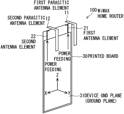
1. A wireless communication device having an antenna configuration in which an omnidirectional antenna element connected to a feeding point is arranged on a printed board, wherein a ground plane connected to a ground potential is formed on the printed board so as to cover an area other than a part where an electronic circuit is formed on the printed board, a parasitic antenna element is arranged at a position adjacent to the omnidirectional antenna element, in a state of being parallel to the omnidirectional antenna element, and the parasitic antenna element is arranged at a position where the parasitic antenna element can receive radio waves reflected on the ground plane, an entire length of the parasitic antenna element is set to be a length that is (½) of a wavelength of radio waves handled by the omnidirectional antenna element,
the parasitic antenna element, at a position by the ground plane and where the parasitic antenna element reaches an edge of the printed board, is bent at a right angle in a direction of approaching the printed board, and
a center position of the parasitic antenna element in a length direction is set at a position where the parasitic antenna element can receive the radio waves reflected on the ground plane.
|