| CPC H01Q 21/0025 (2013.01) [H01Q 21/24 (2013.01); H05K 1/0243 (2013.01); H05K 2201/10098 (2013.01)] | 6 Claims |
|
1. A dual-polarized printed circuit board (PCB) array antenna comprising:
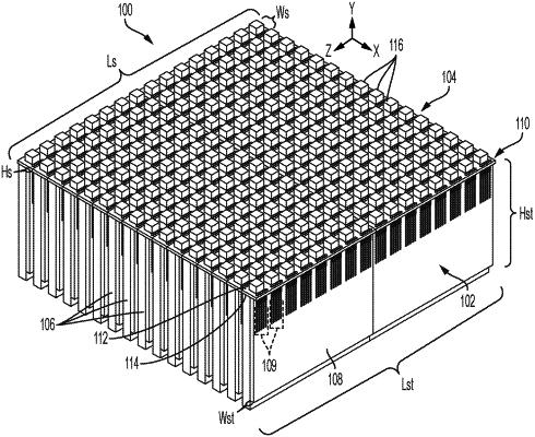
a plurality of PCBs, each PCB extending along a first axis to define a PCB width, a second axis orthogonal to the first axis to define a PCB height, and a third axis orthogonal to the first axis and the second axis to define a PCB length, each PCB having a PCB mounting surface that extends along the second axis from a first PCB end to an opposing second PCB end and along the third axis from a third PCB end to a fourth PCB end,
a radiating antenna array including a plurality of radiator substrates, each radiator substrate having a patch mounting surface that extends along the first axis from a first substrate end to an opposing second substrate end and the third axis from a third substrate end to an opposing fourth substrate end; and
a plurality of orthogonal interfaces configured to arrange the patch mounting surface of a given radiator substrate among the plurality of radiator substrates in an orthogonal position with respect to the PCB mounting surface of a given PCB among the plurality of PCBs,
wherein a given orthogonal interface among the plurality of orthogonal interfaces arranges the patch mounting surface of the given radiator substrate in the orthogonal position with respect to the PCB mounting surface the given PCB, and
wherein the given orthogonal interface comprises:
a plurality of electrically conductive traces formed on the given PCB mounting surface; and
a plurality of electrically conductive pins extending through the patch mounting surface and contacting the electrically conductive traces,
wherein the radiating antenna array includes a plurality of radiating antenna elements disposed on the patch mounting surface.
|