US 11,990,621 B2
Graphene and power storage device, and manufacturing method thereof
Hiroatsu Todoriki, Kanagawa (JP); Yumiko Saito, Kanagawa (JP); Takahiro Kawakami, Kanagawa (JP); Kuniharu Nomoto, Saitama (JP); and Mikio Yukawa, Kanagawa (JP)
Assigned to Semiconductor Energy Laboratory Co., Ltd., Kanagawa-ken (JP)
Filed by SEMICONDUCTOR ENERGY LABORATORY CO., LTD., Atsugi (JP)
Filed on Jun. 2, 2023, as Appl. No. 18/205,264.
Application 18/205,264 is a continuation of application No. 17/983,140, filed on Nov. 8, 2022, granted, now 11,735,731.
Application 17/983,140 is a continuation of application No. 16/935,771, filed on Jul. 22, 2020, abandoned.
Application 16/935,771 is a continuation of application No. 16/599,944, filed on Oct. 11, 2019, abandoned.
Application 16/599,944 is a continuation of application No. 14/507,872, filed on Oct. 7, 2014, granted, now 10,461,332, issued on Oct. 29, 2019.
Application 14/507,872 is a continuation of application No. 13/629,645, filed on Sep. 28, 2012, granted, now 8,883,351, issued on Nov. 11, 2014.
Claims priority of application No. 2011-217897 (JP), filed on Sep. 30, 2011.
Prior Publication US 2023/0307639 A1, Sep. 28, 2023
Int. Cl. H01M 4/583 (2010.01); B82Y 30/00 (2011.01); B82Y 40/00 (2011.01); C01B 32/192 (2017.01); C01B 32/23 (2017.01); H01G 9/042 (2006.01); H01G 11/22 (2013.01); H01G 11/32 (2013.01); H01G 11/36 (2013.01); H01M 4/04 (2006.01); H01M 4/133 (2010.01); H01M 4/139 (2010.01); H01M 4/1393 (2010.01); H01M 4/587 (2010.01); H01M 4/62 (2006.01); H01M 6/16 (2006.01); H01M 10/0566 (2010.01); H01M 10/0525 (2010.01)
CPC H01M 4/5835 (2013.01) [B82Y 30/00 (2013.01); B82Y 40/00 (2013.01); C01B 32/192 (2017.08); C01B 32/23 (2017.08); H01G 9/042 (2013.01); H01G 11/22 (2013.01); H01G 11/32 (2013.01); H01G 11/36 (2013.01); H01M 4/0438 (2013.01); H01M 4/133 (2013.01); H01M 4/139 (2013.01); H01M 4/1393 (2013.01); H01M 4/587 (2013.01); H01M 4/62 (2013.01); H01M 6/16 (2013.01); H01M 10/0566 (2013.01); H01M 10/0525 (2013.01); Y02E 60/13 (2013.01)] 6 Claims
OG exemplary drawing
 
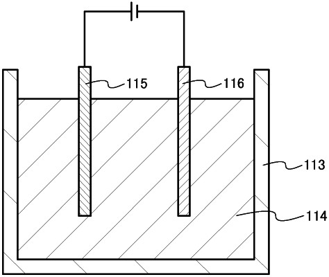
1. A method for manufacturing a power storage device including an electrode, comprising:
forming an active material layer comprising an active material, graphene oxide, and a binder on a current collector; and
electrochemically reducing at least part of the graphene oxide in the active material layer, so as to form graphene comprising an oxygen atom.