| CPC H01M 4/0485 (2013.01) [C22C 24/00 (2013.01); C22F 1/16 (2013.01); H01M 4/02 (2013.01); H01M 4/043 (2013.01); H01M 4/08 (2013.01); H01M 4/134 (2013.01); H01M 4/139 (2013.01); H01M 4/1395 (2013.01); H01M 4/382 (2013.01); H01M 10/052 (2013.01); H01M 2004/021 (2013.01); H01M 2004/027 (2013.01); H01M 2220/30 (2013.01)] | 4 Claims |
|
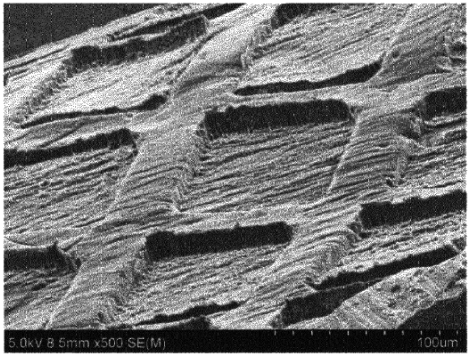
1. A method of patterning a surface of a lithium metal, the method comprising:
forming a uniform intaglio or embossed pattern having a size of 0.001 to 900 μm on a silicon wafer,
wherein the size is a length or a width;
physically pressing a lithium metal to the silicon wafer having the uniform intaglio or embossed pattern formed thereon or applying liquid lithium to the silicon wafer and cooling the liquid lithium in order to form a uniform pattern on a surface of the lithium metal; and
separating the lithium metal having the uniform intaglio or embossed pattern formed thereon from the silicon wafer.
|