| CPC H01L 33/62 (2013.01) [G09G 3/32 (2013.01); H01L 25/0753 (2013.01); H01L 33/005 (2013.01); H01L 33/14 (2013.01); H01L 33/24 (2013.01); G09G 2310/0267 (2013.01); G09G 2310/0275 (2013.01)] | 11 Claims |
|
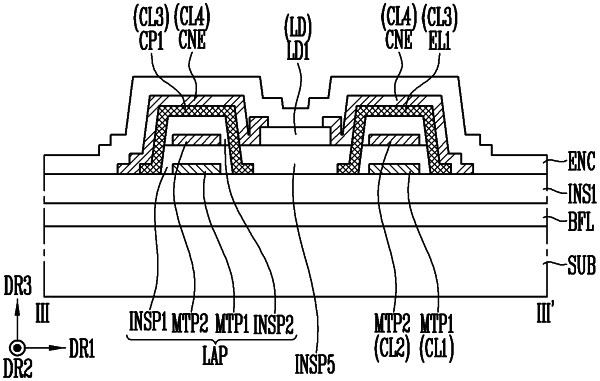
1. A display device comprising:
a substrate comprising:
a display area comprising pixel areas, each pixel area among the pixel areas comprising a first area and a second area;
a non-display area enclosing at least one side of the display area; and
pixels disposed on the pixel areas, each pixel among the pixels comprising light emitting elements,
wherein each pixel among the pixel further comprises:
a pixel circuit part disposed on the first area, the pixel circuit part comprising at least one transistor and at least one capacitor; and
a display element part disposed on the second area, the display element part comprising a first electrode, a second electrode spaced apart from the first electrode, and the light emitting elements disposed between the first electrode and the second electrode,
wherein each of the light emitting elements includes a first end connected to the first electrode, and a second end connected to the second electrode and not overlapping the first end in a plan view,
wherein each of the pixel circuit part and the display element part has a multi-layer structure comprising one or more conductive layers and one or more insulating layers, and
wherein at least one layer of the pixel circuit part and at least one layer of the display element part are disposed in a same layer.
|