| CPC H01L 33/62 (2013.01) [H01L 25/0753 (2013.01); H01L 25/167 (2013.01); H01L 33/647 (2013.01); H01L 2933/0066 (2013.01); H01L 2933/0075 (2013.01)] | 20 Claims |
|
1. A light-emitting device, comprising:
a lead frame having a first surface on which a patterned conductive layer is provided; and
a light-emitting element including:
an insulating substrate formed on said first surface of said lead frame,
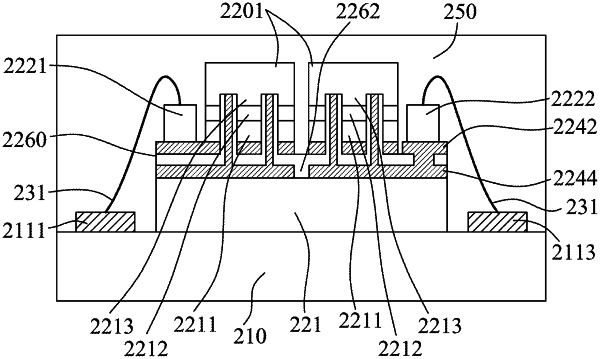
a plurality of light-emitting units formed on said insulating substrate opposite to said lead frame, each of said light-emitting units including a first semiconductor layer, an active layer and a second semiconductor layer that are sequentially disposed on said insulating substrate in such order,
at least one first electrode which is placed in electrical connection with said first semiconductor layer of a first one of said light-emitting units, and which is disposed outward of said light-emitting units; and
at least one second electrode which is placed in electrical connection with said second semiconductor layer of a second one of said light-emitting units, and which is disposed outward of said light-emitting units,
wherein said light-emitting element further includes at least one pair of bonding wires, each of which is disposed to electrically connect a respective one of said first electrode and said second electrode to said patterned conductive layer.
|