| CPC H01L 33/62 (2013.01) [H01L 33/42 (2013.01); H01L 33/44 (2013.01); H01L 33/32 (2013.01); H01L 2933/0025 (2013.01)] | 16 Claims |
|
1. An optoelectronic semiconductor device comprising:
a first semiconductor layer of a first conductivity type;
a second semiconductor layer of a second conductivity type, the first and second semiconductor layers being stacked one on top of the other;
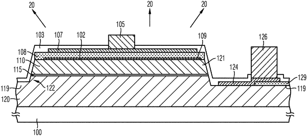
a first contact structure;
a contact layer arranged over a side of the first semiconductor layer facing away from the second semiconductor layer and connected to the first semiconductor layer;
a separating layer arranged over a side of the contact layer facing away from the first semiconductor layer; and
a current spreading layer arranged over a side of the separating layer facing away from the contact layer;
wherein the first contact structure is connected to the contact layer (109) via the current spreading layer and the separating layer;
the separating layer is present as a continuous layer in a region between the contact layer and the current spreading layer and the separating layer has a lower conductivity than the current spreading layer; and
a layer stack comprising the contact layer, the separating layer, and the current spreading layer has an anisotropic conductivity.
|