| CPC H01L 33/60 (2013.01) [H01L 21/78 (2013.01); H01L 33/38 (2013.01); H01L 33/46 (2013.01); H01L 33/54 (2013.01); H01L 33/56 (2013.01)] | 17 Claims |
|
1. A light-emitting device, comprising:
a substrate, comprising a top surface;
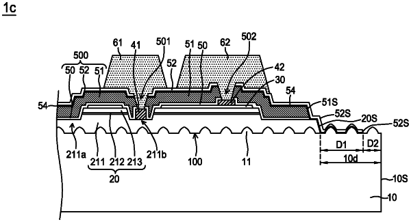
a semiconductor stack formed on the top surface of the substrate, the semiconductor stack comprising a first semiconductor layer, an active layer and a second semiconductor layer, wherein the first semiconductor layer comprises a mesa continuously surrounding a periphery of the semiconductor stack;
a dicing street surrounding the semiconductor stack and exposing the top surface of the substrate; and
an insulating reflective structure comprising a protective layer covering the mesa, a reflective layer comprising a Distributed Bragg Reflector structure covering the protective layer, and a compact layer covering the reflective layer,
wherein the protective layer and the compact layer are in direct contact with each other on the mesa, the reflective layer is formed between the protective layer and the compact layer on the mesa, and the reflective layer does not contact the first semiconductor layer on the mesa.
|