| CPC H01L 33/60 (2013.01) [H01L 21/6835 (2013.01); H01L 25/0753 (2013.01); H01L 33/50 (2013.01); H01L 33/54 (2013.01); H01L 33/58 (2013.01); H01L 2221/68354 (2013.01); H01L 2221/68363 (2013.01); H01L 2933/005 (2013.01); H01L 2933/0058 (2013.01)] | 15 Claims |
|
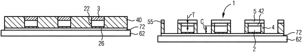
1. A method for producing optoelectronic semiconductor devices, the method comprising:
applying a temporal spacer to protect a light-exit face of an optoelectronic semiconductor chip by:
applying a photoresist onto a first carrier;
subsequently developing the photoresist in places thereby forming the temporal spacer; and
subsequently mounting the optoelectronic semiconductor chip onto a side of the temporal spacer facing away from the first carrier;
forming a reflector in a lateral direction directly around the optoelectronic semiconductor chip and around the temporal spacer;
subsequently removing the temporal spacer so that the reflector extends beyond the light-exit face; and
applying an optical element onto the reflector so that a gap exists between the light-exit face and a light-entrance face of the optical element.
|