| CPC H01L 33/58 (2013.01) [H01L 33/46 (2013.01); H01L 33/507 (2013.01); H01L 33/22 (2013.01); H01L 33/382 (2013.01); H01L 2933/0091 (2013.01)] | 13 Claims |
|
1. A light-emitting diode, comprising:
a substrate;
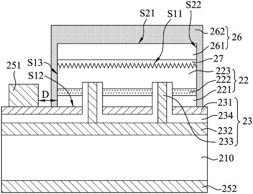
an epitaxial layered structure which is disposed on said substrate and which includes a first-type semiconductor layer, a second-type semiconductor layer, and an active layer sandwiched between said first-type semiconductor layer and said second-type semiconductor layer, said epitaxial layered structure having opposite upper and lower surfaces and a side surface interconnecting said upper and lower surfaces;
a reflective layered unit which is disposed on said lower surface of said epitaxial layered structure;
a light-transmissive structure which covers said upper surface of said epitaxial layered structure and a portion of said side surface of said epitaxial layered structure, and which is configured to allow an emission light emitted from said epitaxial layered structure to exit therefrom at a light-exit angle of not smaller than 125°; and
a first electrode and a second electrode which are electrically connected to said epitaxial layered structure and which are disposed on opposite sides of said substrate,
wherein a light distribution curve of light output from said light-emitting diode is in an oval shape having a maximum length in a longitudinal direction and a maximum width in a transverse direction that is perpendicular to the longitudinal direction, the maximum length being greater than the maximum width,
wherein said light-transmissive structure comprises:
a transparent layer disposed on said upper surface of said epitaxial layered structure, said transparent layer being a sapphire substrate and having a thickness of not less than 30 μm; and
a light conversion layer disposed over said transparent layer, and configured to convert the emission light emitted from said epitaxial layered structure into an excited light having a wavelength different from that of the emission light,
wherein said epitaxial layered structure and said first electrode are spaced apart by a distance so that said light conversion layer is formed on said side surface of said epitaxial layered structure adjacent to said first electrode, and
wherein said first electrode is exposed from said light conversion layer.
|