US 11,990,568 B2
Light emitting device, display device comprising same, and method for manufacturing display device
Young Rag Do, Seoul (KR); and Byung Ju Lee, Seoul (KR)
Assigned to Samsung Display Co., Ltd., Yongin-si (KR)
Appl. No. 17/423,084
Filed by SAMSUNG DISPLAY CO., LTD., Yongin-Si (KR)
PCT Filed Jul. 15, 2019, PCT No. PCT/KR2019/008731
§ 371(c)(1), (2) Date Jul. 14, 2021,
PCT Pub. No. WO2020/149474, PCT Pub. Date Jul. 23, 2020.
Claims priority of application No. 10-2019-0005451 (KR), filed on Jan. 15, 2019.
Prior Publication US 2022/0085247 A1, Mar. 17, 2022
Int. Cl. H01L 33/38 (2010.01); H01L 27/15 (2006.01); H01L 33/00 (2010.01); H01L 33/20 (2010.01); H01L 33/62 (2010.01)
CPC H01L 33/382 (2013.01) [H01L 27/156 (2013.01); H01L 33/005 (2013.01); H01L 33/20 (2013.01); H01L 33/62 (2013.01); H01L 2933/0016 (2013.01)] 20 Claims
OG exemplary drawing
 
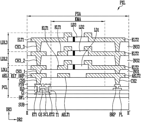
1. A light emitting device, comprising:
a substrate; and
a plurality of light emitting element layers stacked on the substrate,
wherein each of the light emitting element layers comprises:
an insulating layer disposed on an overall surface of the substrate;
a first electrode and a second electrode disposed on the insulating layer and spaced apart from each other; and
a plurality of light emitting elements disposed between the first electrode and the second electrode.