| CPC H01L 33/38 (2013.01) [H01L 21/7806 (2013.01); H01L 25/0753 (2013.01); H01L 33/40 (2013.01); H01L 33/44 (2013.01); H01L 2933/0016 (2013.01); H01L 2933/0025 (2013.01)] | 19 Claims |
|
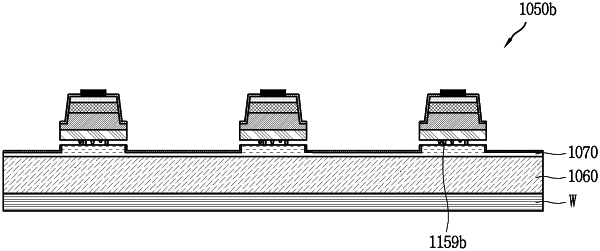
1. A display device comprising:
a plurality of semiconductor light-emitting diodes,
wherein at least one of the plurality of semiconductor light-emitting diodes comprises:
a first conductive electrode and a second conductive electrode;
a first conductive semiconductor layer on which the first conductive electrode is disposed;
a second conductive semiconductor layer that overlaps with the first conductive semiconductor layer, and the second conductive electrode being disposed on the second conductive semiconductor layer;
an active layer disposed between the first conductive semiconductor layer and the second conductive semiconductor layer;
an undoped semiconductor layer disposed on the second conductive semiconductor layer; and
protrusions formed of a porous material allowing electropolishing, and on the undoped semiconductor layer,
wherein a surface on the undoped semiconductor layer has a first region, and a second region that is disposed inward of the first region,
wherein the second region contains the protrusions, and
wherein a surface roughness of the second region is greater than that of the first region.
|