| CPC H01L 33/325 (2013.01) [H01L 33/06 (2013.01)] | 10 Claims |
|
1. A semiconductor light-emitting element having an emission wavelength band with a peak wavelength in an ultraviolet region from 200 nm to 365 nm, the semiconductor light-emitting element comprising:
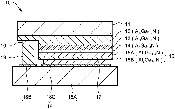
an n-type semiconductor layer that has a composition of AlGaN or AlInGaN;
an active layer formed on the n-type semiconductor layer, the active layer containing an AlGaN semiconductor or an AlInGaN semiconductor;
a p-type semiconductor layer formed on the active layer, the p-type semiconductor layer having a composition of AlN, AlGaN, or AlInGaN; and
a p-electrode formed on the p-type semiconductor layer, the p-electrode being made of metal or metal oxide,
wherein:
the p-type semiconductor layer includes a contact layer formed near an interface between the p-type semiconductor layer and the p-electrode, and the contact layer is an AlGaN layer or an AlInGaN layer in which an Al composition decreases toward the interface between the p-type semiconductor layer and the p-electrode so that a band gap of the contact layer decreases continuously toward the interface between the p-type semiconductor layer and the p-electrode,
the contact layer includes a tunneling contact layer in contact with the p-electrode, and the tunneling contact layer is connected to the p-electrode by a tunnel junction,
a decrease rate of the Al composition in the contact layer toward the interface between the p-type semiconductor layer and the p-electrode is 0.0008 nm−1 to 0.05 nm−1,
the active layer has a quantum well structure that includes a well layer and a barrier layer,
a band gap of the barrier layer is larger than a band gap of the well layer,
the well layer consists of an AlGaN layer having a composition of Alx1Ga1−x1N, and an Al composition of the well layer is 0.5 or greater than 0.5, and
the band gap of the contact layer varies in a band gap range greater than the band gap of the well layer.
|