| CPC H01L 33/145 (2013.01) [H01L 27/156 (2013.01); H01L 33/0062 (2013.01); H01L 33/0095 (2013.01); H01L 33/30 (2013.01)] | 13 Claims |
|
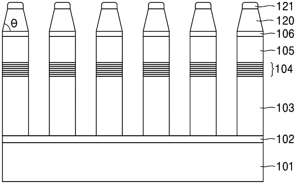
1. A nanorod light emitting device comprising:
a first semiconductor layer doped with a first conductivity type, and comprising a first lower surface and a first upper surface that oppose each other;
a second semiconductor layer doped with a second conductivity type that is electrically opposite to the first conductivity type, and comprising a second lower surface and a second upper surface that oppose each other;
a light emitting layer disposed between the first upper surface of the first semiconductor layer and the second lower surface of the second semiconductor layer; and
a groove formed in a side surface of the second semiconductor layer,
wherein a distance between the first lower surface of the first semiconductor layer and the second upper surface of the second semiconductor layer is in a range of 2 μm to 10 μm,
wherein a difference between a second diameter of the second upper surface of the second semiconductor layer and a first diameter of the first lower surface of the first semiconductor layer is 10% or less of the second diameter of the second upper surface of the second semiconductor layer, and
wherein a third diameter of the groove of the second semiconductor layer is 90% to 95% of the second diameter of the second upper surface of the second semiconductor layer, and
wherein the diameter of the first lower surface of the first semiconductor layer and the diameter of the second upper surface of the second semiconductor layer is from 0.3 μm to 0.5 μm.
|