| CPC H01L 33/06 (2013.01) [H01L 33/0075 (2013.01); H01L 33/32 (2013.01); H01L 33/405 (2013.01); H01L 2933/0016 (2013.01)] | 14 Claims |
|
1. An ultraviolet (UV) light-emitting device comprising:
a substrate having an AluGa1-uN top surface, wherein 0.4≤u≤1.0;
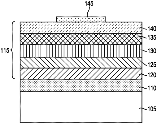
a bottom contact layer disposed over the substrate, the bottom contact layer comprising AlnGa1-nN;
a light-emitting device structure disposed over the bottom contact layer, the device structure comprising a multiple-quantum well layer comprising a plurality of periods each comprising a strained AlxGa1-xN barrier and a strained AlyGa1-yN quantum well, wherein (i) y is less than x by an amount facilitating confinement of charge carriers in the multiple-quantum well layer, and (ii) y is selected such that light emitted by the multiple-quantum well layer has a wavelength of approximately 240 nm or shorter; and
a cap layer disposed over the multiple-quantum well layer, the cap layer comprising AlwGa1-wN, wherein 0≤w≤0.2,
wherein (i) at least a portion of a sidewall of the light-emitting device structure is angled with respect to a normal to the top surface of the substrate at an angle of approximately a Brewster angle of the light emitted by the multiple-quantum well layer, (ii) the light-emitting device structure is disposed within a mesa disposed over the substrate, at least a portion of the mesa having the sidewall angle, and (iii) the device further comprises a conductive bottom contact disposed over the bottom contact layer and around at least a portion of a base of the mesa.
|