| CPC H01L 33/025 (2013.01) [H01L 33/0095 (2013.01); H01S 5/04256 (2019.08); H01S 5/34333 (2013.01); H01L 33/007 (2013.01); H01L 33/0075 (2013.01); H01L 33/20 (2013.01); H01L 33/32 (2013.01)] | 20 Claims |
|
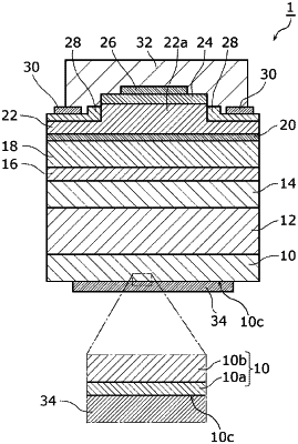
1. A nitride-based semiconductor light-emitting element, comprising: a first n-type nitride-based semiconductor layer including a group IV n-type impurity; and
an n-side electrode in contact with the first n-type nitride-based semiconductor layer, wherein
the first n-type nitride-based semiconductor layer includes
a surface layer region in contact with the n-side electrode, the surface layer region including a halogen element, and
an internal region located across the surface layer region from the n-side electrode,
a peak concentration of the group IV n-type impurity in the surface layer region is at least 1.0×1021 cm−3,
a peak concentration of the halogen element in the surface layer region is at least 10% of the peak concentration of the group IV n-type impurity in the surface layer region, and
a concentration of the group IV n-type impurity in the internal region is lower than a concentration of the group IV n-type impurity in the surface layer region.
|