| CPC H01L 33/0095 (2013.01) [H01L 25/0753 (2013.01); H01L 2933/0058 (2013.01); H01L 2933/0066 (2013.01)] | 17 Claims |
|
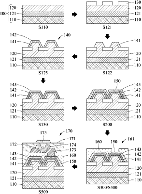
1. A method of manufacturing a micro-light emitting diode (LED)-based display, the method comprising:
forming a micro-LED partitioned in the unit of a plurality of sub-pixels in a micro-LED region of a semiconductor substrate;
forming a current spreading layer on a p-type semiconductor layer of the micro-LED, wherein a portion of the current spreading layer extends into a thin-film transistor region (TFT region) of the semiconductor substrate, the TFT region positioned adjacent the micro-LED region,
planarizing the micro-LED by forming a planarization layer on at least a portion of the micro-LED and on the portion of the current spreading layer that extends into the TFT region;
forming a via hole in the planarization layer so that the portion of the current spreading layer that extends into the TFT region is exposed; and
integrating the micro-LED and a thin-film transistor (TFT) for an operation of the sub-pixels by arranging and depositing the TFT at least partially over the TFT region and inserting a drain region of the TFT into the via hole to contact the portion of the current spreading layer that extends into the TFT region.
|