| CPC H01L 31/143 (2013.01) [H01L 27/14625 (2013.01); H01L 31/0203 (2013.01); H01L 31/02325 (2013.01); H01L 31/186 (2013.01)] | 8 Claims |
|
1. An optical sensor package, comprising:
an optical sensor chip, the optical sensor chip comprising:
a base layer;
a light detection region, arranged in the base layer; and
a light source, arranged on and electrically coupled to the base layer;
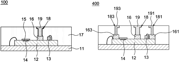
a first light blocking wall, arranged on the base layer of the optical sensor chip, and located between the light detection region and the light source, the first light blocking wall extending in a first direction and having an upper surface extending in the first direction, wherein the upper surface has an inner portion extending in the first direction and an outer portion surrounding the entire inner portion in a second direction perpendicular to the first direction;
a transparent layer, disposed on the optical sensor chip and the first light blocking wall, wherein the transparent layer has a groove exposing the first light blocking wall, and an upper part of the groove has a first width, and a lower part of the groove has a second width smaller than the first width; and
a second light blocking wall, filled in the groove and stacked on the first light blocking wall, wherein a bottom part of the second light blocking wall is stacked only on the inner portion of the upper surface of the first light blocking wall.
|