| CPC H01L 31/0352 (2013.01) [G01S 7/4865 (2013.01); G01S 17/06 (2013.01); G01S 17/894 (2020.01); H01L 27/14643 (2013.01)] | 14 Claims |
|
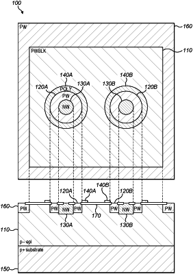
1. A photonic mixer device for multiplying an impinging optical signal with a reference electrical signal, the photonic mixer device comprising:
a semiconductor substrate of a first conductivity type,
two detector regions of a second conductivity type different from the first conductivity type,
two biasing regions of the first conductivity type with a higher dopant concentration than the dopant concentration of the semiconductor substrate, each biasing region positioned near one of the respective detector regions, wherein an electrical field can be formed in the semiconductor substrate by applying a voltage bias between the biasing regions,
two bias electrodes, which are isolated from the substrate and the biasing regions, wherein each bias electrode is only locally, partially or completely, covering an outer edge of one of the respective biasing regions, such that when biasing the bias electrodes with a bias voltage, the bias voltage is only local just over the outer edge of the biasing regions and such that the bias electrodes are covering charge pockets which are present in an electrostatic potential between the biasing regions underneath the outer edges of the biasing regions.
|