| CPC H01L 31/022425 (2013.01) [H01L 31/02167 (2013.01)] | 19 Claims |
|
1. A solar cell, comprising:
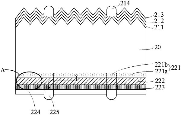
a substrate;
an interface passivation layer on a rear surface of the substrate, wherein the interface passivation layer includes a first interface passivation sub-layer and a second interface passivation sub-layer;
at least one electrode disposed at a side of the interface passivation layer facing away from the substrate, the first interface passivation sub-layer corresponding to a portion of the interface passivation layer between adjacent electrodes, and the second interface passivation sub-layer corresponding to a portion of the interface passivation layer between the substrate and the at least one electrode;
a field passivation layer, at least partially disposed between the interface passivation layer and the at least one electrode; and
a conductivity enhancement layer, at least partially disposed at a side of the first interface passivation sub-layer facing away from the substrate, and configured to enable carriers in the first interface passivation sub-layer to flow to the at least one electrode, wherein a resistivity of a material of the conductivity enhancement layer is smaller than a resistivity of a material of the field passivation layer, and the resistivity of the material of the conductivity enhancement layer is smaller than 0.0010 Ω·cm;
wherein the conductivity enhancement layer covers a surface of the interface passivation layer facing away from the substrate, the field passivation layer covers a surface of the conductivity enhancement layer facing away from the substrate, and the at least one electrode is configured to contact with the field passivation layer.
|