| CPC H01L 29/872 (2013.01) [H01L 29/0619 (2013.01); H01L 29/66143 (2013.01); H01L 29/868 (2013.01)] | 12 Claims |
|
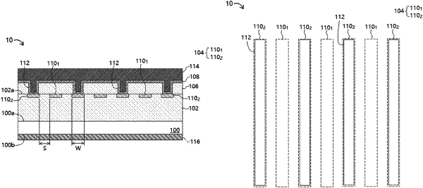
1. A merged PiN Schottky (MPS) diode, comprising:
a substrate having a first surface and a second surface opposite to the first surface;
a first epitaxial layer of a first conductivity type disposed on the first surface of the substrate;
a plurality of doped regions of a second conductivity type disposed in a surface of the first epitaxial layer, wherein the doped regions consist of first portions and second portions, the first portions are electrically floating, and the second portions are electrically connected to a top metal;
a second epitaxial layer of the first conductivity type disposed on the surface of the first epitaxial layer, wherein a plurality of trenches is formed in the second epitaxial layer to expose the second portions of the doped regions; and
a Schottky metal layer conformally deposited on the second epitaxial layer and the exposed second portions of the doped regions.
|