| CPC H01L 29/78618 (2013.01) [H01L 27/1225 (2013.01); H01L 27/124 (2013.01); H01L 27/1259 (2013.01); H01L 29/7869 (2013.01)] | 5 Claims |
|
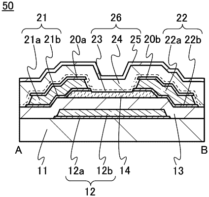
1. A semiconductor device comprising:
a semiconductor film;
a first electrode electrically connected to the semiconductor film and functioning as one of a source electrode and a drain electrode;
a second electrode electrically connected to the semiconductor film and functioning as the other of the source electrode and the drain electrode;
a first protective film between a first film of the first electrode and the semiconductor film;
a second protective film between a second film of the second electrode and the semiconductor film;
a third protective film over the first film;
a fourth protective film over the second film;
an insulating film over the third protective film, the fourth protective film, and the semiconductor film;
a third electrode functioning as a gate electrode; and
a fifth protective film below a third film of the third electrode,
wherein each of the first film and the second film comprises copper,
wherein the third protective film has a first region, a second region, and a third region,
wherein the fourth protective film has a fourth region, a fifth region, and a sixth region,
wherein the first region extends outward beyond a first side surface of the first film,
wherein the third region extends outward beyond a second side surface of the first film,
wherein the second region overlaps with the first film,
wherein the fourth region extends outward beyond a first side surface of the second film,
wherein the sixth region extends outward beyond a second side surface of the second film,
wherein the fifth region overlaps with the second film,
wherein the insulating film is in contact with the first region, the second region, the third region, the fourth region, the fifth region, and the sixth region,
wherein a top surface of the insulating film is not planarized,
wherein the fifth protective film has a seventh region and an eighth region,
wherein the seventh region extends outward beyond a first side surface of the third film,
wherein the eighth region extends outward beyond a second side surface of the third film,
wherein the seventh region overlaps with the second region,
wherein the eighth region overlaps with the fifth region, and
wherein each of the third protective film and the fourth protective film comprises a light-transmitting conductive film.
|