| CPC H01L 29/7856 (2013.01) [H01L 21/0217 (2013.01); H01L 21/0228 (2013.01); H01L 21/3065 (2013.01); H01L 21/3105 (2013.01); H01L 21/31116 (2013.01); H01L 21/32 (2013.01); H01L 21/76897 (2013.01); H01L 21/823431 (2013.01); H01L 21/823821 (2013.01); H01L 27/0886 (2013.01); H01L 29/0649 (2013.01); H01L 29/0847 (2013.01); H01L 29/66553 (2013.01); H01L 29/66795 (2013.01); H01L 29/66803 (2013.01); H01L 21/823814 (2013.01); H01L 29/66545 (2013.01)] | 20 Claims |
|
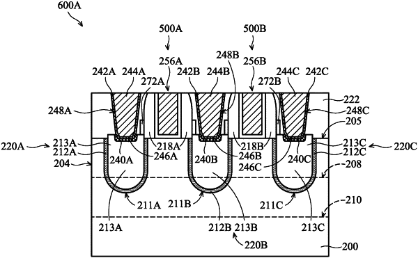
1. A semiconductor structure, comprising:
a gate structure formed over a fin structure, wherein the gate structure comprises a gate dielectric layer;
a source/drain (S/D) epitaxial layer formed in the fin structure and adjacent to the gate structure;
a S/D silicide layer formed on the S/D epitaxial layer, wherein the S/D silicide layer has a first width, the S/D epitaxial layer has a second width, and the first width is smaller than the second width; and
a dielectric spacer between the gate structure and the S/D silicide layer, wherein a top surface of the dielectric spacer is lower than a top surface of the gate structure, and an interface between the dielectric spacer and the S/D epitaxial layer is higher than a bottommost surface of the gate dielectric layer, wherein a topmost surface of the gate dielectric layer is higher than a top surface of the dielectric spacer.
|