| CPC H01L 29/785 (2013.01) [H01L 27/0886 (2013.01); H01L 29/0649 (2013.01); H01L 29/41791 (2013.01); H01L 29/66795 (2013.01); H01L 2029/7858 (2013.01)] | 14 Claims |
|
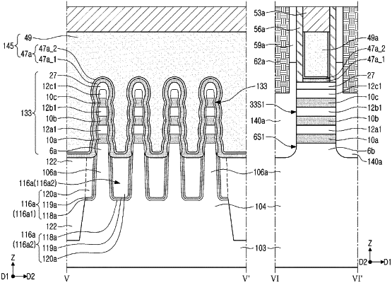
1. A semiconductor device, comprising:
active regions on a substrate;
a first isolation region on side surfaces of the active regions and on the substrate;
source/drain regions on the active regions;
fin structures on the active regions, the source/drain regions being in contact with first side surfaces of the fin structures in a first direction; and
a gate structure on the fin structures and the first isolation region,
wherein the gate structure covers second side surfaces of the fin structures in a second direction and upper surfaces of the fin structures, the second direction being perpendicular to the first direction, and the first direction and the second direction being parallel to an upper surface of the substrate,
wherein each of the fin structures includes:
a stack structure having first semiconductor layers and second semiconductor layers that alternate and are stacked in a vertical direction, the vertical direction being perpendicular to the upper surface of the substrate, and
a semiconductor capping layer that covers side surfaces of the stack structure in the second direction,
wherein the first semiconductor layers include a material different from a material of the second semiconductor layers, and
wherein a width in the second direction of a central portion of at least one of the second semiconductor layers is greater than a width in the second direction of a central portion of at least one of the first semiconductor layers.
|