| CPC H01L 29/785 (2013.01) [H01L 29/0847 (2013.01); H01L 29/41775 (2013.01); H01L 29/41791 (2013.01); H01L 29/6656 (2013.01); H01L 29/66795 (2013.01)] | 17 Claims |
|
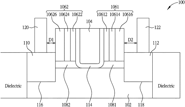
17. A transistor with low leakage currents, comprising:
a substrate;
a gate formed above a gate dielectric layer;
a spacer, wherein the spacer comprises at least two sublayers;
a pad dielectric layer formed under the spacer, wherein a bottom of each sublayer of the spacer completely contacts with the pad dielectric layer; and
a source region or a drain region, wherein the source region or the drain region is adjacent to the spacer;
wherein the gate dielectric layer has a bottom directly contacted with the substrate and has a curved corner contacted with the pad dielectric layer, and a maximum width between two most lateral edges of the curved corners of the gate dielectric layer is not greater than a width between two most lateral edges of sidewalls of the gate dielectric layer.
|