| CPC H01L 29/7848 (2013.01) [H01L 21/0245 (2013.01); H01L 29/16 (2013.01)] | 5 Claims |
|
1. A semiconductor device, comprising:
a gate structure on a substrate; and
epitaxial layers adjacent to two sides of the gate structure, wherein the each of the epitaxial layers comprises:
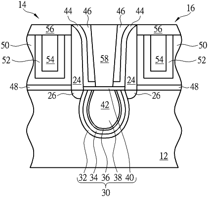
a buffer layer directly contacting the substrate;
a first linear bulk layer on and directly contacting a top surface of the buffer layer, wherein the first linear bulk layer is a single layer having a single concentration gradient and even thickness;
a second linear bulk layer on the first linear bulk layer, wherein a maximum thickness of the second linear bulk layer is less than a maximum and a minimum thickness of the first linear bulk layer, a top surface of the second linear bulk layer is even with top surfaces of the substrate and the first linear bulk layer, a germanium (Ge) concentration of the buffer layer is less than a Ge concentration of the first linear bulk layer, the Ge concentration of the first linear bulk layer is less than a Ge concentration of the second linear bulk layer, a slope of the Ge concentration of the buffer layer is zero, a slope of the Ge concentration of the first linear bulk layer is less than a slope of the Ge concentration of the second linear bulk layer, and the slope of the Ge concentration of the first linear bulk layer is a single slope; and
a bulk layer on the second linear bulk layer, wherein the buffer layer, the first linear bulk layer, the second linear bulk layer, and the bulk layer are made of silicon germanium (SiGe) and a slope of the Ge concentration of the bulk layer is not zero.
|