| CPC H01L 29/7816 (2013.01) [H01L 29/1095 (2013.01); H01L 29/402 (2013.01); H01L 29/42368 (2013.01)] | 20 Claims |
|
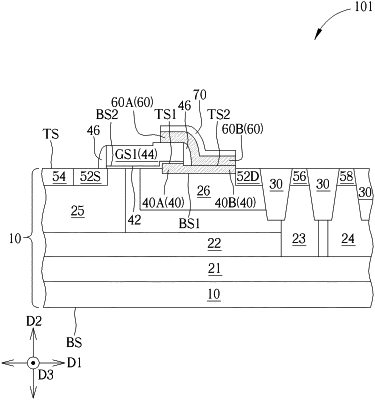
1. A semiconductor device, comprising:
a semiconductor substrate;
a gate structure disposed on the semiconductor substrate;
a gate dielectric layer disposed between the gate structure and the semiconductor substrate in a vertical direction;
a source region and a drain region disposed in the semiconductor substrate and located at two opposite sides of the gate structure in a horizontal direction respectively;
a first oxide layer comprising:
a first portion disposed between the gate structure and the semiconductor substrate in the vertical direction; and
a second portion disposed between the gate structure and the drain region;
a field plate partly disposed above the gate structure and partly disposed above the second portion of the first oxide layer; and
a second oxide layer comprising:
a first portion disposed between the field plate and the gate structure in the vertical direction, wherein a part of the gate dielectric layer is located under the first portion of the second oxide layer in the vertical direction and located above the first portion of the first oxide layer in the vertical direction; and
a second portion disposed between the field plate and the second portion of the first oxide layer in the vertical direction, wherein a projection pattern of the field plate in the vertical direction is identical to a projection pattern of the second oxide layer in the vertical direction.
|