US 11,990,545 B2
Semiconductor device having fully oxidized gate oxide layer and method for making the same
Tsu-Hsiu Perng, Hsinchu (TW); Yun-Chi Wu, Hsinchu (TW); Chia-Chen Chang, Hsinchu (TW); Cheng-Bo Shu, Hsinchu (TW); Jyun-Guan Jhou, Hsinchu (TW); and Pei-Lun Wang, Hsinchu (TW)
Assigned to TAIWAN SEMICONDUCTOR MANUFACTURING COMPANY, LTD., Hsinchu (TW)
Filed by TAIWAN SEMICONDUCTOR MANUFACTURING COMPANY, LTD., Hsinchu (TW)
Filed on Oct. 19, 2022, as Appl. No. 17/969,180.
Application 17/969,180 is a continuation of application No. 17/332,002, filed on May 27, 2021, granted, now 11,508,843.
Prior Publication US 2023/0040514 A1, Feb. 9, 2023
This patent is subject to a terminal disclaimer.
Int. Cl. H01L 21/00 (2006.01); H01L 21/02 (2006.01); H01L 29/06 (2006.01); H01L 29/66 (2006.01); H01L 29/78 (2006.01)
CPC H01L 29/7816 (2013.01) [H01L 21/0214 (2013.01); H01L 21/0223 (2013.01); H01L 29/0611 (2013.01); H01L 29/66681 (2013.01)] 20 Claims
OG exemplary drawing
 
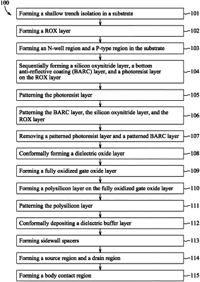
1. A method for making a semiconductor device, comprising:
forming a patterned silicon oxynitride layer on a substrate;
conformally forming a dielectric oxide layer to cover the substrate and the patterned silicon oxynitride layer; and
fully oxidizing the patterned silicon oxynitride layer to form a fully oxidized gate oxide layer on the substrate.