| CPC H01L 29/7813 (2013.01) [H01L 29/407 (2013.01); H01L 29/78642 (2013.01)] | 20 Claims |
|
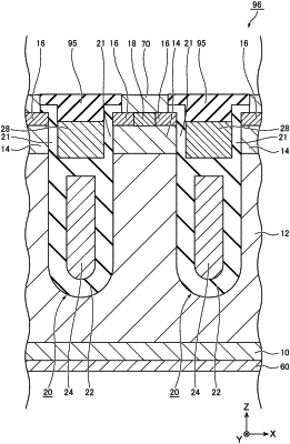
1. A semiconductor device comprising:
a first electrode; and
a substrate including a first surface in contact with the first electrode and a second surface provided opposite to the first surface, the first surface including a first groove including a first length and a second length shorter than the first length, the first length in a first direction parallel to the first surface, the second length in a second direction parallel to the first surface, the second direction intersecting with the first direction, wherein
the substrate includes
a semiconductor layer having a first conductive type,
a first semiconductor region provided between the semiconductor layer and the second surface, the first semiconductor region having a second conductive type,
a second semiconductor region provided between the first semiconductor region and the second surface, the second semiconductor region having an impurity concentration of the first conductive type higher than an impurity concentration of the semiconductor layer, and
a plurality of second electrodes provided in the first direction, the plurality of second electrodes being provided opposite to the first semiconductor region in a first insulating film on the substrate,
wherein the first groove overlaps with the plurality of second electrodes in a third direction intersecting with the first direction and the second direction.
|