| CPC H01L 29/7788 (2013.01) [H01L 29/2003 (2013.01); H01L 29/205 (2013.01); H01L 29/7789 (2013.01); H01L 29/7802 (2013.01)] | 4 Claims |
|
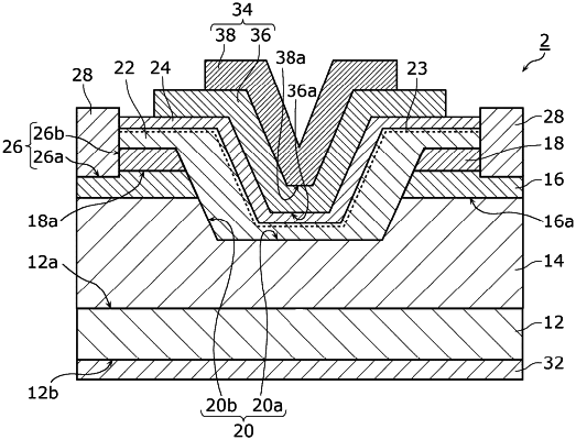
1. A nitride semiconductor device, comprising:
a substrate;
a first nitride semiconductor layer above the substrate, the first nitride semiconductor layer being of an n-type;
a second nitride semiconductor layer above the first nitride semiconductor layer, the second nitride semiconductor layer being of a p-type;
a first opening which penetrates through the second nitride semiconductor layer to the first nitride semiconductor layer;
an electron transport layer and an electron supply layer disposed on an inner face of the first opening, in the stated order from a side on which the substrate is located;
a gate electrode above the electron supply layer and covering the first opening;
a second opening at a position distanced from the first opening, the second opening penetrating through the electron supply layer and the electron transport layer to the second nitride semiconductor layer;
a source electrode covering the second opening, the source electrode being connected to the electron supply layer, the electron transport layer, and the second nitride semiconductor layer; and
a drain electrode on a side of the substrate opposite from a side of the substrate on which the first nitride semiconductor layer is located,
wherein a bottom face of the gate electrode is closer to the drain electrode than a bottom face of the second nitride semiconductor layer is, and
wherein the gate electrode includes:
a metal layer including a metal material; and
a third nitride semiconductor layer between the metal layer and the electron supply layer, the third nitride semiconductor layer being of a p-type,
wherein a bottom face of the third nitride semiconductor layer is closer to the drain electrode than the bottom face of the second nitride semiconductor layer is.
|