| CPC H01L 29/7786 (2013.01) [H01L 29/2003 (2013.01); H01L 29/205 (2013.01); H01L 29/401 (2013.01); H01L 29/41775 (2013.01); H01L 29/66462 (2013.01)] | 18 Claims |
|
1. A semiconductor device, comprising:
a substrate;
a semiconductor channel layer disposed on the substrate;
a semiconductor barrier layer disposed on the semiconductor channel layer;
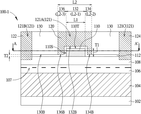
a gate capping layer disposed on the semiconductor barrier layer, wherein the gate capping layer comprises a top surface, a first sidewall, and a second sidewall opposite to the first sidewall;
a dielectric layer conformally covering the gate capping layer and surrounding a periphery of the gate capping layer, wherein the top surface of the gate capping layer is completely covered with the dielectric layer in a top view;
a gate electrode disposed on the dielectric layer, completely covering the dielectric layer on the top surface and the first sidewall of the gate capping layer and exposing the dielectric layer on the second sidewall of the gate capping layer, wherein the gate electrode is completely separated from the gate capping layer by the dielectric layer, and a top surface of the gate capping layer contacts the dielectric layer, wherein the top surface of the gate capping layer is completely covered with the gate electrode in a top view; and
a source electrode and a drain electrode respectively disposed in a source contact hole and a drain contact hole, wherein the source contact hole and the drain contact hole are disposed in the semiconductor barrier layer, and bottom surfaces of the source contact hole and the drain contact hole are disposed between a top surface and a bottom surface of the semiconductor barrier layer so as to expose the semiconductor barrier layer.
|