| CPC H01L 29/7397 (2013.01) [H01L 29/42324 (2013.01)] | 7 Claims |
|
1. An insulated gate bipolar transistor (IGBT) device, comprising:
an n-type collector region and a p-type collector region, an n-type drift region located above the n-type collector region and the p-type collector region, a plurality of p-type body regions located at a top of the n-type drift region, and at least one first MOSFET cell and at least one second MOSFET cell;
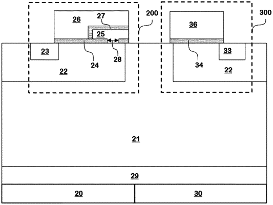
wherein each first MOSFET cell of the at least one first MOSFET cell comprises: a first n-type emitter region located within each p-type body region of the plurality of p-type body regions; a first gate structure located above the each p-type body region, wherein the first gate structure comprises a first gate dielectric layer, a first gate and an n-type floating gate both located above the first gate dielectric layer, wherein the n-type floating gate is located on a side close to the n-type drift region in a lateral direction and the first gate is located on a side close to the first n-type emitter region and extends over the n-type floating gate; an insulating dielectric layer located between the n-type floating gate and the first gate; and an opening located in the first gate dielectric layer, wherein the n-type floating gate is in contact with the each p-type body region through the opening to form a p-n junction diode; and
wherein each second MOSFET cell of the at least one second MOSFET cell comprises a second n-type emitter region located within the each p-type body region and configured to control ON and OFF of a current channel located between the second n-type emitter region and the n-type drift region, wherein the second gate structure comprises a second gate dielectric layer and a second gate.
|