| CPC H01L 29/7371 (2013.01) [H01L 29/0817 (2013.01); H01L 29/0821 (2013.01); H01L 29/1004 (2013.01); H01L 29/66242 (2013.01)] | 20 Claims |
|
1. A heterojunction bipolar transistor, comprising:
a substrate;
a bottom sub-collector layer disposed on the substrate;
an upper sub-collector layer disposed on the bottom sub-collector layer;
a collector layer disposed on the upper sub-collector layer;
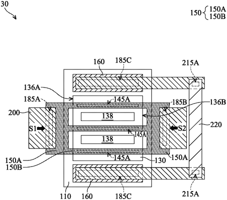
a base layer disposed on the collector layer, wherein the base layer, the collector layer and the upper sub-collector layer form a base mesa, and wherein in a top view, the base layer comprises a first side and a second side opposite to the first side;
an emitter layer disposed on the base layer;
a first dielectric film disposed on the bottom sub-collector layer and the base mesa;
a base electrode disposed on the first dielectric film and connected to the base layer through a first via hole disposed in the first dielectric film;
a second dielectric film disposed on the base electrode; and
a first conductive layer disposed on the second dielectric film, wherein the first conductive layer is connected to the base electrode through a second via hole disposed in the second dielectric film at the first side of the base layer, the first conductive layer is connected to the base electrode through a third via hole disposed in the second dielectric film at the second side of the base layer, and the second via hole and the third via hole are laterally spaced away from the base layer.
|