| CPC H01L 29/737 (2013.01) [H01L 27/0623 (2013.01); H01L 29/0821 (2013.01); H01L 29/66242 (2013.01)] | 16 Claims |
|
1. A method of manufacturing a heterojunction bipolar transistor, comprising:
forming a semiconductor collector region in a substrate by:
forming a lower collector layer within the substrate;
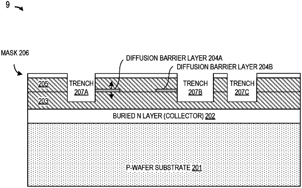
forming a barrier layer above the lower collector layer such that the barrier layer is configured to impede diffusion of dopants from the lower collector layer through the barrier layer during one or more subsequent manufacturing steps, wherein the barrier layer is located at peripheral sides of the semiconductor collector region, separate from a center of the semiconductor collector region; and
forming an upper collector layer above the barrier layer;
forming a trench isolation region in the substrate that electrically insulates the semiconductor collector region, wherein the barrier layer is adjacent to the trench isolation region;
selectively forming a heterogeneous base region on a portion of the semiconductor collector region by forming a heterogeneous stack of semiconductor layers; and
selectively forming an emitter region on a portion of the heterogeneous base region.
|