| CPC H01L 29/737 (2013.01) [H01L 21/02532 (2013.01); H01L 21/2251 (2013.01); H01L 29/0808 (2013.01); H01L 29/0817 (2013.01); H01L 29/0821 (2013.01); H01L 29/1008 (2013.01); H01L 29/165 (2013.01); H01L 29/66242 (2013.01)] | 20 Claims |
|
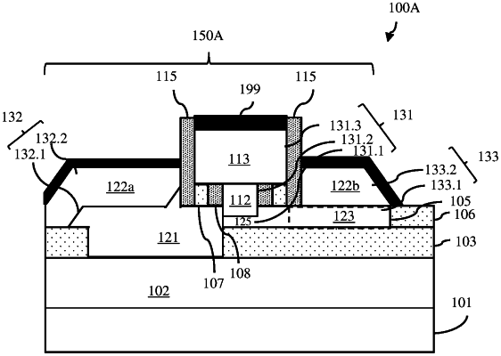
1. A structure comprising:
a substrate comprising a first semiconductor material;
an insulator layer on the substrate;
a semiconductor layer on the insulator layer, wherein the semiconductor layer comprises a second semiconductor material different from the first semiconductor material; and
a transistor comprising:
a base on the insulator layer, the base comprising:
a first base region within the semiconductor layer;
a second base region on the first base region and comprising the second semiconductor material; and
a third base region on the second base region;
a collector; and
an emitter, wherein the base is positioned laterally between the collector and the emitter and wherein at least one of the collector and the emitter comprises:
a first region within a trench that extends through the semiconductor layer and the insulator layer to the substrate, wherein the first region comprises an upper surface above an upper surface of the first base region; and
a second region on the first region.
|