| CPC H01L 29/732 (2013.01) [H01L 21/82285 (2013.01); H01L 21/823821 (2013.01); H01L 29/063 (2013.01); H01L 29/0649 (2013.01); H01L 29/6656 (2013.01); H01L 29/735 (2013.01)] | 19 Claims |
|
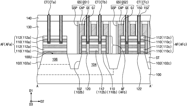
1. A method for manufacturing semiconductor devices, comprising:
forming a well region in a substrate;
forming a first active fin and a second active fin on the well region;
forming trenches in the substrate to define a first active pattern and a second active pattern in the well region, wherein the first active fin and the second active fin are on the first active pattern and the second active pattern, respectively;
forming device isolation patterns in the trenches;
forming an impurity region in the first active pattern;
forming a plurality of sacrificial gate structures running across the second active fin, each of the plurality of sacrificial gate structures including,
a sacrificial gate electrode running across the second active fin, and
a plurality of gate spacers on lateral surfaces of the sacrificial gate electrode;
removing the second active fin between the plurality of sacrificial gate structures to expose the second active pattern;
forming a connection pattern on the second active pattern between a corresponding pair of the plurality of sacrificial gate structures and connected to the well region; and
forming a first contact plug on the connection pattern and between the corresponding pair of a plurality of gate structures such that lateral surfaces of a portion of an upper part of the first contact plug are in direct contact with corresponding ones of the plurality of gate spacers, respectively, wherein each of the plurality of gate structures is formed by replacing the sacrificial gate electrode with a gate electrode,
wherein the forming an impurity region includes implanting the first active fin and the first active pattern with impurities having a first conductivity type, and
wherein the substrate has the first conductivity type and the well region includes impurities having a second conductivity type different from the first conductivity type.
|