US 11,990,533 B2
Tunneling field effect transistor and semiconductor device including the same
MinCheol Shin, Daejeon (KR); YeongJun Lim, Daejeon (KR); and Junbeom Seo, Daejeon (KR)
Assigned to Korea Advanced Institute Of Science And Technology, Daejeon (KR)
Filed by KOREA ADVANCED INSTITUTE OF SCIENCE AND TECHNOLOGY, Daejeon (KR)
Filed on Mar. 22, 2022, as Appl. No. 17/701,195.
Claims priority of application No. 10-2021-0037091 (KR), filed on Mar. 23, 2021.
Prior Publication US 2022/0310828 A1, Sep. 29, 2022
Int. Cl. H01L 29/73 (2006.01); H01L 29/739 (2006.01)
CPC H01L 29/7311 (2013.01) [H01L 29/7391 (2013.01)] 20 Claims
OG exemplary drawing
 
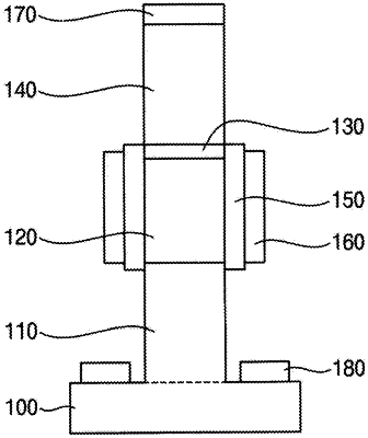
1. A tunneling field effect transistor (TFET), comprising:
a drain region on a substrate;
a channel on the drain region;
a dipole formation layer (DFL) on the channel;
a source region on the DFL;
a gate insulation pattern surrounding the channel; and
a gate electrode surrounding the gate insulation pattern,
wherein the DFL contacts the channel and the source region and forms dipoles between the channel and the source region.