| CPC H01L 29/66742 (2013.01) [B82Y 10/00 (2013.01); H01L 21/823487 (2013.01); H01L 21/823885 (2013.01); H01L 29/0676 (2013.01); H01L 29/068 (2013.01); H01L 29/0847 (2013.01); H01L 29/1033 (2013.01); H01L 29/42392 (2013.01); H01L 29/66439 (2013.01); H01L 29/775 (2013.01); H01L 29/78642 (2013.01); H01L 29/78681 (2013.01); H01L 29/78684 (2013.01); H01L 29/78696 (2013.01); H01L 21/02381 (2013.01); H01L 21/0245 (2013.01); H01L 21/02532 (2013.01)] | 20 Claims |

|
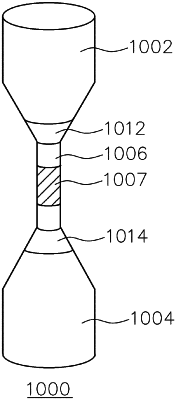
1. A method of forming a vertical transistor structure, the method comprising:
receiving a substrate;
forming a source/drain region;
forming a channel, wherein the source/drain region and the channel are stacked in a vertical direction relative to the substrate; and
forming a junction, wherein:
a cross-sectional diameter of the junction continuously varies in an increasing manner in the vertical direction from a cross-sectional diameter of the channel to a cross-sectional diameter of the source/drain region to connect the source/drain region to the channel without a stepwise transition between the cross-sectional diameter of the channel and the cross-sectional diameter of the source/drain region; and
at least a portion of the source/drain region has a cross-sectional diameter that varies such that a portion of the source/drain region closest to the substrate is different than a portion of the source/drain region furthest from the substrate.
|