| CPC H01L 29/66522 (2013.01) [H01L 21/02532 (2013.01); H01L 21/02546 (2013.01); H01L 21/02609 (2013.01); H01L 21/3065 (2013.01); H01L 29/42392 (2013.01); H01L 29/66469 (2013.01); H01L 29/6653 (2013.01); H01L 29/78696 (2013.01); H01L 29/66545 (2013.01)] | 20 Claims |

|
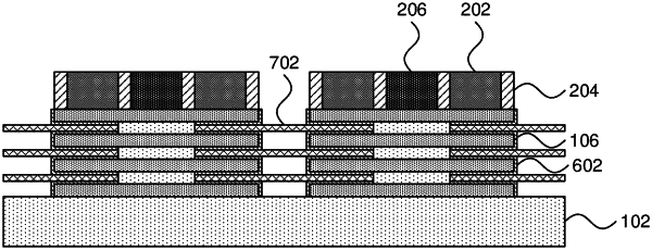
1. A method for forming a semiconductor device, comprising:
recessing first sacrificial layers relative to second sacrificial layers in a stack of alternating first and second sacrificial layers;
growing replacement channel layers from sidewalls of the first sacrificial layers;
growing source/drain regions from the replacement channel layers;
etching away the first sacrificial layers and the second sacrificial layers; and
forming a gate stack between, around, and in direct contact with the replacement channel layers and in contact with upper and lower surfaces of the replacement channel layers.
|
|
10. A method for forming a semiconductor device, comprising:
recessing first sacrificial layers relative to second sacrificial layers in a stack of alternating first and second sacrificial layers;
forming a protective layer on the second sacrificial layers by depositing a layer of conversion material and annealing the layer of conversion material;
growing replacement channel layers from sidewalls of the first sacrificial layers;
growing source/drain regions from the replacement channel layers;
etching away the first sacrificial layers and the second sacrificial layers; and
forming a gate stack between, around, and in direct contact with the replacement channel layers and in contact with upper and lower surfaces of the replacement channel layers.
|
|
17. A method for forming a semiconductor device, comprising:
growing a stack of alternating first and second sacrificial layers from a substrate having a top surface with a (110) crystal orientation;
recessing first sacrificial layers relative to second sacrificial layers in the stack of alternating first and second sacrificial layers;
growing replacement channel layers from sidewalls of the first sacrificial layers, wherein the sidewalls of the first sacrificial layers have a (111) crystal orientation;
growing source/drain regions from the replacement channel layer;
etching away the first and second sacrificial layers; and
forming a gate stack between, around, and in direct contact with the replacement channel layers and in contact with upper and lower surfaces of the replacement channel layers.
|