| CPC H01L 29/4991 (2013.01) [H01L 21/02603 (2013.01); H01L 21/28123 (2013.01); H01L 21/764 (2013.01); H01L 29/0673 (2013.01); H01L 29/42392 (2013.01); H01L 29/66545 (2013.01); H01L 29/66553 (2013.01); H01L 29/66636 (2013.01); H01L 29/66742 (2013.01); H01L 29/78618 (2013.01); H01L 29/78696 (2013.01)] | 20 Claims |
|
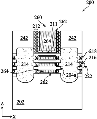
1. A method, comprising:
forming a dummy gate stack over a fin;
forming an S/D recess in the fin;
depositing a first spacer layer within the S/D recess, wherein the depositing forms a plurality of air gaps in the first spacer layer, and wherein each of the plurality of air gaps is surrounded by the first spacer layer;
before forming an epitaxial source/drain (S/D) feature, removing portions of the first spacer layer adjacent the fin while maintaining the plurality of air gaps surrounded by the first spacer layer; and
forming the epitaxial S/D feature in the S/D recess and laterally adjacent to the first spacer layer having the plurality of air gaps.
|