| CPC H01L 29/42364 (2013.01) [H01L 29/401 (2013.01); H01L 29/51 (2013.01); H01L 29/512 (2013.01); H01L 29/518 (2013.01); H01L 29/66712 (2013.01); H01L 29/7802 (2013.01)] | 15 Claims |
|
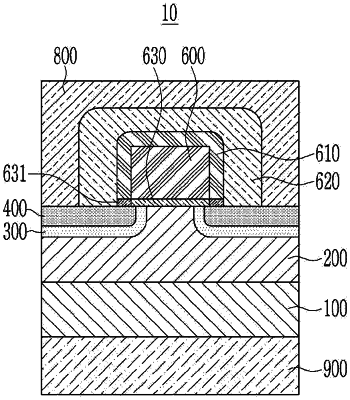
12. A method of manufacturing a semiconductor device, the method comprising:
forming an n− type layer, and a p type region on a first surface of a substrate;
forming a gate on the n− type layer;
forming a first gate protection layer on the gate;
forming a second gate protection layer on the first gate protection layer;
forming a source on the second gate protection layer and the p type region; and
forming a drain on a second surface of the substrate,
wherein the forming of the gate includes forming a gate insulating layer on the n− type layer, forming a gate material layer on the gate insulating layer, and etching the gate material layer to form the gate,
wherein the forming of the first gate protection layer includes forming the first gate protection layer on the gate, and etching a portion of the gate insulating layer which is not protected by the first gate protection layer, using the first gate protection layer as a mask, to remove the portion of the gate insulating layer, and
wherein the gate insulating layer includes a conductive polymer by etching using an etching gas.
|