| CPC H01L 29/4236 (2013.01) [H01L 27/088 (2013.01); H01L 29/78 (2013.01)] | 20 Claims |
|
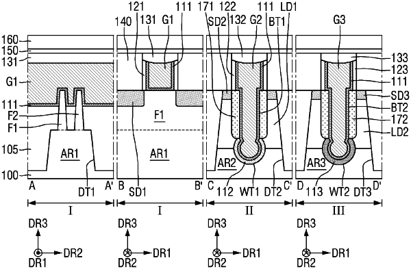
1. A semiconductor device comprising:
an active region extending in a first horizontal direction on a substrate;
source/drain regions disposed on the active region;
a buried trench formed between the source/drain regions;
a buried insulating layer surrounding both side walls of the buried trench in the first horizontal direction between the source/drain regions;
a wing trench formed in a lower part of the buried trench and having a width greater than a width of the buried trench; and
a gate electrode extending in a second horizontal direction on the active region, and disposed within each of the buried trench and the wing trench.
|