| CPC H01L 29/41775 (2013.01) [H01L 29/401 (2013.01); H01L 29/66545 (2013.01)] | 20 Claims |

|
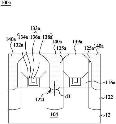
1. A method of forming a semiconductor device, comprising:
forming a dummy gate structure across a fin protruding from a substrate, wherein the dummy gate structure has a dummy gate dielectric layer and a dummy gate electrode over the dummy gate dielectric layer;
forming gate spacers on opposite sidewalls of the dummy gate structure;
forming source/drain epitaxial structures on opposite sides of the dummy gate structure;
performing a first etch process to the dummy gate electrode such that a recessed dummy gate electrode remains over the fin;
performing a second etch process to the gate spacers such that recessed gate spacers remain along the opposite sidewalls of the dummy gate structure;
removing the recessed dummy gate electrode and the dummy gate dielectric layer after the second etch process to form a recess between the recessed gate spacers;
forming a metal gate structure overfilling the recess, wherein forming the metal gate structure comprises:
forming a fill metal layer filling the recess, wherein the fill metal layer has a top width and a bottom width less than the top width, wherein the fill metal layer has a middle portion having a width decreasing in a direction toward the fin; and
performing a third etch process to the metal gate structure such that a recessed metal gate structure remains between the recessed gate spacers.
|