| CPC H01L 29/404 (2013.01) [H01L 21/765 (2013.01); H01L 29/407 (2013.01); H01L 29/66734 (2013.01); H01L 29/7813 (2013.01)] | 9 Claims |
|
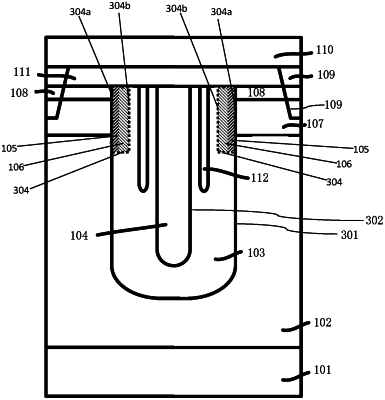
1. A shield gate trench (SGT) MOSFET device, wherein a gate structure thereof comprises:
a gate trench, a shielding dielectric layer, a source conductive material layer, a second field plate conductive material layer, and a gate conductive material layer;
the shielding dielectric layer is formed on an inner side surface of the gate trench, and the shielding dielectric layer encloses an intermediate trench in the gate trench;
the source conductive material layer fills the intermediate trench;
the second field plate conductive material layer is formed in a first top sub-trench at both sides of the source conductive material layer, and the gate conductive material layer is formed in a second top sub-trench at both sides of the source conductive material layer;
the first top sub-trench and the second top sub-trench are both formed in the shielding dielectric layer;
a depth of the first top sub-trench is greater than a depth of the second top sub-trench, and the first top sub-trench is located between the source conductive material layer and the second top sub-trench in a lateral direction;
a first side surface of the second top sub-trench is on a corresponding side surface of the gate trench, and the gate conductive material layer and the first side surface of the second top sub- trench are spaced apart by a gate dielectric layer provided therebetween;
the second field plate conductive material layer fully fills the first top sub-trench;
the gate trench is formed in a first epitaxial layer of a first conductivity type, a doped channel region of a second conductivity type is formed in a surface region of the first epitaxial layer, and the second top sub-trench penetrates through the channel region;
the first epitaxial layer at the bottom of the channel region forms a drift region, and a heavily doped source region of the first conductivity type is formed on the surface of the channel region;
a heavily doped drain region of the first conductivity type is formed on the backside surface of the first epitaxial layer; and
when the device is reversely biased, in a longitudinal direction from the drain region to the bottom surface of the channel region, a voltage of the drift region gradually decreases, a voltage difference between the source conductive material layer and the drift region gradually decreases, and depletion capability with respect to the drift region at a side close to the channel region is enhanced due to the feature that a spacing between the second field plate conductive material layer and the drift region is less than a spacing between the source conductive material layer and the drift region.
|