| CPC H01L 29/2206 (2013.01) [C01G 15/006 (2013.01); H01L 21/0242 (2013.01); H01L 21/02433 (2013.01); H01L 21/02483 (2013.01); H01L 21/02496 (2013.01); H01L 29/78 (2013.01); H01L 21/0262 (2013.01); H01L 29/7395 (2013.01); H01L 29/7786 (2013.01)] | 15 Claims |
|
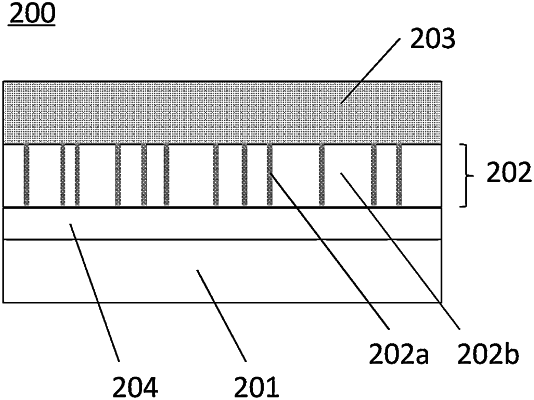
1. A laminate comprising:
a crystal substrate;
a middle layer formed on a main surface of the crystal substrate, the middle layer comprising a mixture of an amorphous region in an amorphous phase and a crystal region in a crystal phase having a corundum structure mainly made of a first metal oxide; and
a crystal layer formed on the middle layer and having a corundum structure mainly made of a second metal oxide,
wherein the crystal region is an epitaxially grown layer from a crystal plane of the crystal substrate,
the middle layer further comprises silicon, and
a silicon concentration in the middle layer is 0.5 at % or more.
|