| CPC H01L 29/1608 (2013.01) [H01L 21/02378 (2013.01); H01L 21/565 (2013.01); H01L 21/78 (2013.01); H01L 23/3114 (2013.01); H01L 23/544 (2013.01)] | 21 Claims |

|
1. A method of manufacturing a semiconductor device, the method comprising:
providing a silicon carbide substrate that comprises a plurality of device regions and a grid- shaped kerf region laterally separating the device regions;
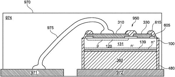
forming a mold structure from a mold material that includes glass, ceramic or a polymer-based material, on a backside surface of the grid-shaped kerf region which faces an opposite direction as a front side surface of the silicon carbide substrate and in which the device regions are formed;
forming backside metal structures on a backside surface of the device regions which faces the same direction as the backside surface of the grid-shaped kerf region and the opposite direction as the front side surface in which the device regions are formed;
separating the device regions; and
prior to forming the mold structure, providing an auxiliary structure that comprises stencil sections,
wherein the stencil sections are provided on the backside surface of the device regions and each stencil section is assigned to one device region,
wherein the mold structure fills a space between the stencil sections,
wherein parts of the mold structure form frame structures laterally surrounding the backside metal structures.
|