| CPC H01L 29/1608 (2013.01) [H01L 27/0255 (2013.01); H01L 29/4933 (2013.01); H01L 29/7804 (2013.01); H01L 29/7813 (2013.01)] | 18 Claims |
|
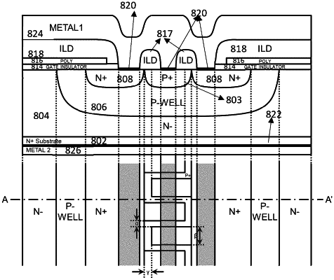
1. A device comprising a unit cell on a Silicon Carbide (SiC) substrate, the unit cell comprising:
a first conductivity type source region on the SiC substrate;
a second conductivity type well region that contains the first conductivity type source region;
and
a silicide layer interrupted by interlayer dielectric (ILD) regions on the SiC substrate,
wherein the device comprises a vertical Silicon Carbide double-implantation metal oxide semiconductor field-effect transistor (DMOSFET) comprising a drain terminal and a source terminal on the SiC substrate,
wherein the source terminal is located on a first side of the SiC substrate and the drain terminal is located on a second side of the SiC substrate,
wherein the source terminal is in contact with the silicide layer,
wherein a second conductivity type well contact region meanders within the second conductivity type well region to form a periodic contact region with the source terminal through the silicide layer, and
wherein the periodic contact region provides reduced contact area.
|